
浏览历史
相关文章
商品描述
商品属性
商品标签
相关商品
相关配件
购买过此商品的人还购买过
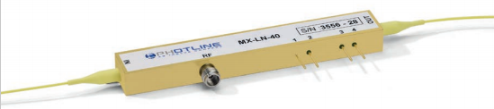
1550nm强度调制器
The Photline MX-LN series are lithium niobate (LiNbO3) intensity modulators designed for optical communications at data rates up to 44 Gb/s.
The X-cut design of these Mach-Zehnder modulators confer them an unmatched stability in a wide range of operational conditions, as well as a zero chirp performance. Ixblue proprietary waveguide design offers a low insertion loss combined with a high contrast. The MX-LN series are ideally suited for 10 Gb/s up to 44 Gb/s optical transmission with NRZ, RZ, DPSK, Duo Binary modulation formats and are key device for a large variety of high bandwidth applications.
FEATURES
• High bandwidth
• X-cut for high stability
• Low drive voltage
• Low insertion loss
APPLICATIONS
• Digital communications
• General purpose intensity modulation
• Test and measurement
OPTIONS
• High extinction ratio versions
• 2000 nm, 1300 nm, 1060 nm, 850 nm
RELATED EQUIPMENTS
• RF amplifiers
• MBC-DG Automatic Bias Controllers
• ModBox-CBand-NRZ
MX-LN-10 Performance Highlights
Parameter
Min
Typ
Max
Unit
Operating wavelength
1530
-
1625
nm
Insertion loss
-
2.7
3
dB
Electro-optical bandwidth
10
12
-
GHz
Vp RF @50 kHz
-
5.5
-
V
Specifications given at 25 °C, 1550 nm
MX-LN-20 Performance Highlights
Parameter
Min
Typ
Max
Unit
Operating wavelength
1530
-
1625
nm
Insertion loss
-
3.5
-
dB
Electro-optical bandwidth
20
25
-
GHz
Vp RF @50 kHz
-
5
-
V
Specifications given at 25 °C, 1550 nm
MX-LN-40 Performance Highlights
Parameter
Min
Typ
Max
Unit
Operating wavelength
1530
-
1625
nm
Insertion loss
-
3.5
-
dB
Electro-optical bandwidth
28
30
-
GHz
Vp RF @50 kHz
-
5
-
V
Specifications given at 25 °C, 1550 nm
MX-LN-10
10 GHz Intensity modulator
Electrical Characteristics
Parameter
Symbol
Condition
Min
Typ
Max
Unit
Electro-optic bandwidth
S21
RF electrodes, from 2 GHz
10
12
-
GHz
Ripple S21
DS21
RF electrodes, f < 12 GHz
-
0.5
1
dB
Electrical return loss
S11
RF electrodes
-
-12
-10
dB
Vp RF @50 kHz
VpRF50 kHz
RF electrodes, @1550 nm
-
5.5
6.5
V
Vp RF @10 Gb/s PRBS
VpRF10 Gb/s
RF electrodes, @1550 nm
-
6.5
7
V
Vp DC electrodes
VpDC
DC electrodes
-
6.5
7
V
RF input impedance
Zin-RF
-
-
50
-
W
DC input impedance
Zin-DC
-
-
1
-
MW
50 W RF input
Optical Characteristics
Parameter
Symbol
Condition
Min
Typ
Max
Unit
Crystal
-
-
Lithium Niobate X-Cut Y-Prop
Operating wavelength
l
-
1530
1550
1625
nm
Insertion loss
IL
Without connectors
-
2.7
3
dB
DC extinction ratio
ER
Measured with narrow source
linewidth < 200 MHz
20
22
-
dB
Optical return loss
ORL
-
-40
-45
-
dB
Chirp
a
-
-0.1
0
0.1
-
All specifications given at 25°C, 1550 nm, unless differently specified
Absolute Maximum Ratings
Stresses in excess of the absolute maximum ratings can cause permanent damage to the device. These are absolute stress ratings only. Functional operation of the device is not implied at these or any other conditions in excess of those given in the operational sections of the data sheet. Exposure to absolute maximum ratings for extended periods can adversely affect device reliability.
Parameter
Symbol
Min
Max
Unit
RF input power
EPin
-
28
dBm
Bias voltage
Vbias
-20
+20
V
Optical input power
OPin
-
20
dBm
Operating temperature
OT
0
+70
°C
Storage temperature
ST
-40
+85
°C
MX-LN-20
20 GHz Intensity modulator
Electrical Characteristics
Parameter
Symbol
Condition
Min
Typ
Max
Unit
Electro-optic bandwidth
S21
RF electrodes, from 2 GHz
20
25
-
GHz
Ripple S21
DS21
RF electrodes, f < 20 GHz
-
0.5
1
dB
Electrical return loss
S11
RF electrodes
-
-12
-10
dB
Vp RF @50 kHz
VpRF50 kHz
RF electrodes, @1550 nm
-
5
5.5
V
Vp RF @20 Gb/s PRBS
VpRF20 Gb/s
RF electrodes, @1550 nm
-
5.5
6
V
Vp DC electrodes
VpDC
DC electrodes
-
6.5
7
V
RF input impedance
Zin-RF
-
-
50
-
W
DC input impedance
Zin-DC
-
-
1
-
MW
50 W RF input
Optical Characteristics
Parameter
Symbol
Condition
Min
Typ
Max
Unit
Crystal
-
-
Lithium Niobate X-Cut Y-Prop
Operating wavelength
l
-
1530
1550
1625
nm
Insertion loss
IL
Without connectors
-
3.5
4.5
dB
DC extinction ratio
ER
Measured with narrow source
linewidth < 200 MHz
20
22
-
dB
Optical return loss
ORL
-
-40
-45
-
dB
Chirp
a
-
-0.1
0
0.1
-
All specifications given at 25 °C, 1550 nm, unless different specified
Absolute Maximum Ratings
Stresses in excess of the absolute maximum ratings can cause permanent damage to the device. These are absolute stress ratings only. Functional operation of the device is not implied at these or any other conditions in excess of those given in the operational sections of the data sheet. Exposure to absolute maximum ratings for extended periods can adversely affect device reliability.
Parameter
Symbol
Min
Max
Unit
RF input power
EPin
-
28
dBm
Bias voltage
Vbias
-20
+20
V
Optical input power
OPin
-
20
dBm
Operating temperature
OT
0
+70
°C
Storage temperature
ST
-40
+85
°C
MX-LN-40
40 GHz Intensity modulator
Electrical Characteristics
Parameter
Symbol
Condition
Min
Typ
Max
Unit
Electro-optic bandwidth
S21
RF electrodes, from 2 GHz
28
30
-
GHz
Ripple S21
DS21
RF electrodes, f < 30 GHz
-
0.5
1
dB
Electrical return loss
S11
RF electrodes
-
-12
-10
dB
Vp RF @50 kHz
VpRF50 kHz
RF electrodes, @1550 nm
-
5
6
V
Vp DC electrodes
VpDC
DC electrodes, @1550 nm
-
6.5
7
V
RF input impedance
Zin-RF
-
-
50
-
W
DC input impedance
Zin-DC
-
1
-
-
MW
50 Ω RF input
Optical Characteristics
Parameter
Symbol
Condition
Min
Typ
Max
Unit
Crystal
-
-
Lithium Niobate X-Cut Y-Prop
Operating wavelength
l
-
1530
1550
1625
nm
Insertion loss
IL
Without connectors
-
3.5
4.5
dB
DC extinction ratio
ER
Measured with narrow source
linewidth < 200 MHz
20
22
-
dB
Optical return loss
ORL
-
-40
-45
-
dB
Chirp
a
-
-0.1
0
0.1
-
All specifications given at 25 °C, 1550 nm, unless different specified
Absolute Maximum Ratings
Stresses in excess of the absolute maximum ratings can cause permanent damage to the device. These are absolute stress ratings only. Functional operation of the device is not implied at these or any other conditions in excess of those given in the operational sections of the data sheet. Exposure to absolute maximum ratings for extended periods can adversely affect device reliability.
Parameter
Symbol
Min
Max
Unit
RF input power
EPin
-
28
dBm
Bias voltage
Vbias
-20
+20
V
Optical input power
OPin
-
20
dBm
Operating temperature
OT
0
+70
°C
Storage temperature
ST
-40
+85
°C
MX-LN-10 Typical S21 Curve MX-LN-10 Typical S11 Curve
MX-LN-20 Typical S21 Curve MX-LN-20 Typical S11 Curve
MX-LN-40 Typical S21 Curve MX-LN-40 Typical S11 Curve
Mechanical Diagram and Pinout
All measurements in mm
Port
Function
Note
IN
Optical input port
Polarization maintaining fiber, Corning PM 15-U25D,
Length 1.5 meter. Buffer diameter 900 mm
OUT
Optical output port
Polarization maintaining fiber, Corning PM 15-U25D,
Length 1.5 meter. Buffer diameter 900 mm
RF
RF input port
MX-LN-10: Wiltron female K (SMA compatible)
MX-LN-20: Wiltron female K or V (optional)
MX-LN-40: Wiltron female V
1
Ground
Pin feed through diameter 1.0 mm
2
DC
Pin feed through diameter 1.0 mm
3, 4
Photodiode cathode, anode
Pin feed through diameter 1.0 mm
Ordering information
MX-LN-BW-XX-Y-Z-AB-CD
BW = Bandwidth : 10 10 GHz 20 20 GHz 40 40 GHz
XX = Internal photodiode : 00 Not integrated PD PD Integrated
Y = Input fiber : P Polarization maintaining S Standard single mode
Z = Output fiber : P Polarization maintaining S Standard single mode
AB = Intput connector : 00 bare fiber FA FC/APC FC FC/SPC
CD = Output connector : 00 bare fiber FA FC/APC FC FC/SPC
Note : optical connectors are Seikoh-Giken with narrow key or equivalent


商品属性 [操作波长] 1530nm-1625nm [带宽] 25GHz [插入损耗] 3.5dB

报价需求
返回顶部
© 2015-2024 神科仪购网/SNKOO-eGo 版权所有,并保留所有权利。
广州番禺区亚运大道1003号番山总部E谷3栋805 Tel: 020-84050812/13/16 ICP备案证书号:粤ICP备14034210号-1